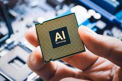
Nvidia is reportedly pouring billions of dollars into expanding advanced chip-packaging capacity at a Taiwanese supplier as severe manufacturing bottlenecks threaten to slow the delivery of high-performance artificial intelligence (AI) processors. The move comes as the global race to build AI infrastructure has unleashed unprecedented capital into advanced packaging – a stage of semiconductor manufacturing once viewed as routine, but now standing as the primary choke point in producing next-generation hardware.
Supply cracks at TSMC force chipmakers to look elsewhereTaiwan Semiconductor Manufacturing Company (TSMC) currently dominates the market for the most sophisticated packaging technologies, primarily Chip-on-Wafer-on-Substrate (CoWoS). This method mounts individual silicon dies, such as processors and high-bandwidth memory, onto a shared base so they can transfer data at high speeds.
CoWoS is essential for processors designed by Nvidia, AMD and Broadcom, as well as custom silicon created by major cloud providers. However, TSMC’s limited packaging capacity has left chip designers scrambling to find alternatives.
To bypass the squeeze, Nvidia is providing billions of dollars in financing to expand CoWoS capacity at Siliconware Precision Industries (SPIL), a subsidiary of Taiwan’s ASE Technology, news agency Reuters cited an industry executive familiar with the situation, as saying. Notably, Nvidia is not alone in funding external capacity. Rival AMD has announced plans to invest more than $10 billion across Taiwan’s semiconductor ecosystem, striking partnerships with ASE, SPIL and Powertech Technology.
“I think CoWoS and advanced packaging are super important for our high-performance computing going forward. TSMC has been an incredible partner in advanced packaging, and we're going to continue to do more together. And yes, we do need more capacity overall,” AMD CEO Lisa Su told Reuters during an October visit to Taipei.
Why packaging now commands half the valueFor decades, packaging was an afterthought aimed at encasing chips in plastic or ceramic to protect them and connect them to circuit boards. “Packaging was always that thing that you just didn't worry about,” former Intel CEO Pat Gelsinger, now a partner at Playground Global, said recently in Taipei. That dynamic has flipped as shrinking transistors onto single silicon slabs becomes increasingly difficult and expensive. Today's GPUs and CPUs frequently combine anywhere from 10 to 20 distinct chips into a single package. Gelsinger estimates advanced packaging could eventually account for as much as half of a chip’s total value.
AI chips rely heavily on this integration because training and running large models requires immense amounts of data to move between compute dies and memory banks without delay.
The rise of panel-level packagingTSMC’s tight lines have created major openings for secondary packaging firms like Taiwan’s Powertech Technology (PTI).
“Everyone is looking for a solution outside TSMC. They don't want to rely entirely on TSMC,” Powertech Chairman D.K. Tsai said in August.
PTI is betting on panel-level packaging, which processes chips on wide rectangular panels instead of conventional round silicon wafers. The format fits more units per run and cuts material waste – a key benefit as AI chips grow physically larger.
PTI is collaborating with AMD and Broadcom to prove the viability of panel packaging for large-scale AI applications. Powertech also plans to invest $400 million in an advanced packaging joint venture with Broadcom in Singapore, targeting production by 2028.
Contact to : xlf550402@gmail.com
Copyright © boyuanhulian 2020 - 2023. All Right Reserved.